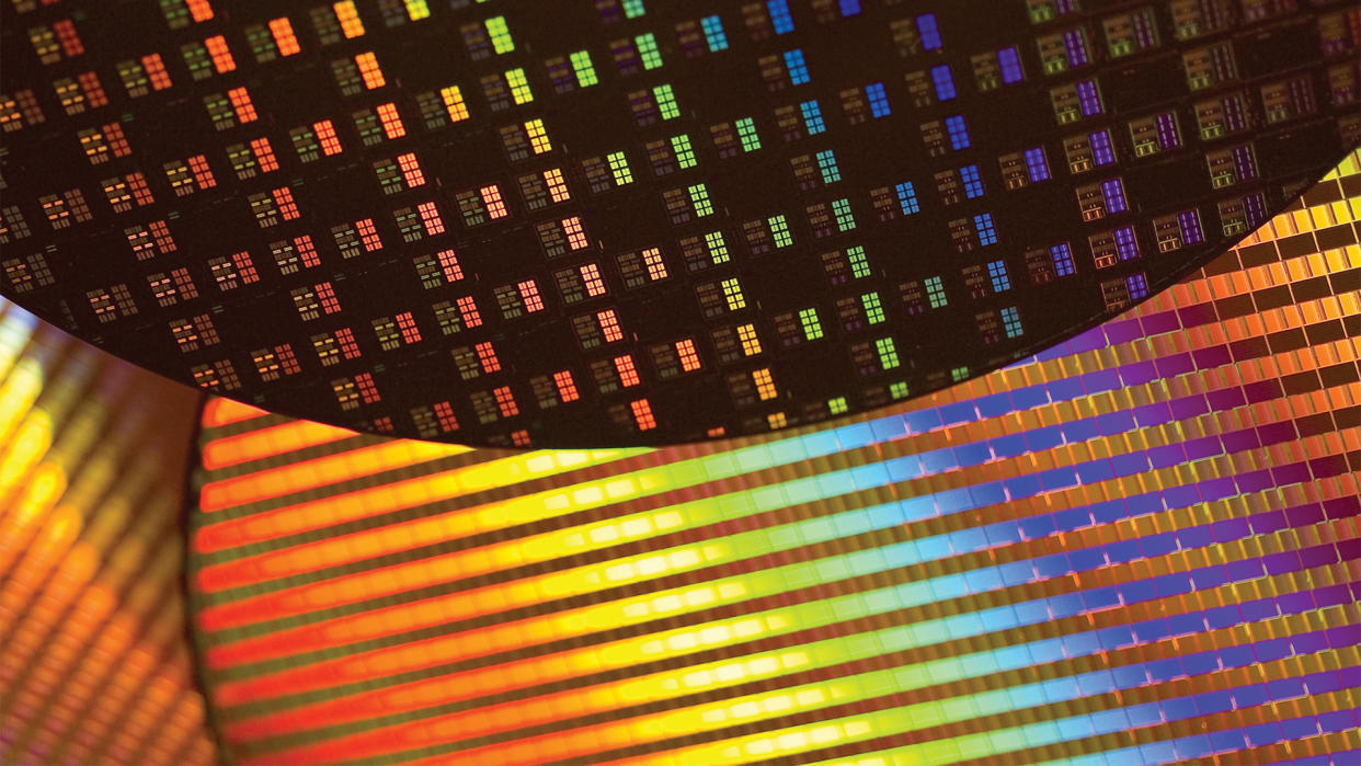
TSMC's third generation 3nm node on track — N3P mass production to begin later this year
TSMC successfully started production of chips on its second generation 3nm-class process technology in the fourth quarter of 2023, meeting its planned milestones. The company is now preparing for mass production of chips on the performance-enhanced version of this node, N3P. This should occur in the second half of 2024, TSMC announced at the European Technology Symposium.
The N3E process entered volume production as scheduled, achieving defect densities comparable to N5 technology when it entered mass production in 2020. That's a good result as TSMC managed to meet the demand from Apple and Huawei back them. TSMC describes its N3E yields as 'great,' which is perhaps evident as the only processor to use N3E for now — Apple's M4 — increased both the number of transistors and operational clockspeed compared to N3-based M3.
"N3E started volume production in the fourth quarter of last year, as planned," a TSMC executive said at the event. "We have seen great yield performance on customers' products, so they did go to market as planned."
A key detail of the N3E process is its simplification relative to TSMC's original N3 process (aka N3B). By removing some layers that required EUV lithography and completely avoiding usage of EUV double patterning, N3E reduces production costs as well as widens the process window and improves yields. These changes, however, sometimes reduce transistor density and power efficiency, a tradeoff that can been mitigated by design optimizations.
Looking ahead, the N3P process provides an optical shrink of the N3E, and it's showing promising progress as well. It has passed essential qualifications and shows yield performance nearing that of N3E. This next evolution in TSMC's technology portfolio aims to boost performance by up to 4% or cut power usage by about 9% at the same clock speeds, while also enhancing transistor density by 4% for chips with mixed design configurations.
N3P maintains compatibility with the N3E's IP blocks, design tools, and methodologies, making it an attractive option for developers. This continuity ensures that most new chip designs (tape outs) are expected to transition from using N3E to N3P, leveraging the latter's improved performance and cost-efficiency.
The final readiness of N3P for production is scheduled for the latter half of this year, when it enters the HVM (high volume manufacturing) stage. TSMC anticipates immediate adoption by chip designers. Given its advantages in performance and cost, N3P is poised to become popular among TSMC's customers, including Apple and AMD.
While the precise timing for the market debut of N3P-based chips remains uncertain, it's anticipated that major players like Apple will use this technology for its 2025 processor lineup. That includes SoCs for smartphones, PCs, and tablets.
"We have also successfully delivered N3P technology," the TSMC executive said. "It has passed qualification and yield performance is close to N3E. [The process technology] has also received product customer tape outs and will start on production in the second half of this year. Because of [PPA advantages] of N3P, we expect the majority of tape outs on N3 to go to N3P."

