TSMC readies lower-cost 4nm manufacturing tech: Up to 8.5% cheaper
TSMC has unveiled its new 4 nm-class production technology, N4C, a new fabrication process set to enhance the company's 5nm-class production nodes by offering significant cost reductions and optimizing design efficiency.
"We are not done with our 5nm and 4nm [technologies]," said Kevin Zhang, Vice President of Business Development at TSMC, at the company's North American Technology Symposium 2024, where the new process was revealed. "From N5 to N4, we have achieved 4% density improvement optical shrink, and we continue to enhance the transistor performance. Now we bring in N4C to our 4 nm technology portfolio. N4C allows our customers to reduce their costs by removing some of the masks and to also improve on the original IP design like a standard cell and SRAM to further reduce the overall product level cost of ownership."
The N4C process technology is a part of TSMC’s N5/N4 node family and builds on the N4P technology. By redesigning the standard cell and SRAM cell, altering some design rules, and decreasing the number of masking layers used, TSMC plans to cut costs by up to 8.5%. These changes not only simplify the manufacturing process but also reduce the size of the dies, which could potentially improve yield due to less complexity and smaller area requirements.
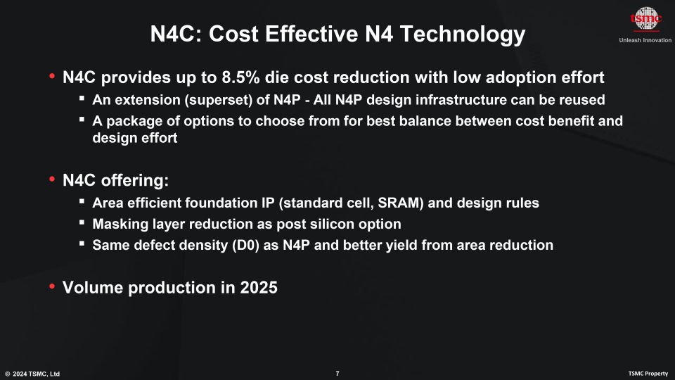
This cost-effective node uses the same design infrastructure as N4P, although it is still unclear whether IP from N5, N4, and N4P can be directly transferred to N4C-based chips. This introduces some uncertainty regarding compatibility with existing designs. We don't yet know how easy it will be to port them to N4C from N5 or N4. TSMC implies that it is going to offer the best balance between cost-benefit and design effort, with a view to encouraging the adoption of its N4C process, but the details remain to be seen.
The introduction of N4C is strategically important for TSMC as it provides a way for customers to significantly lower their production costs for a 4nm-class node, which may drive the adoption of this process technology among customers looking for relatively low costs. The new node promises a well-adjusted combination of power, performance, and area (PPA), making it an attractive option for many of TSMC's clients.
Given the high costs associated with 3nm-class technologies and their relatively limited advantages over nodes like N4P in terms of performance and transistor density, N4C is positioned to be a popular choice.
TSMC expects to start producing chips using the N4C technology in 2025. With six years of experience in 5 nm-class fabrication processes by then, the company anticipates that N4C will achieve good yields and maintain lower costs, reinforcing its appeal as a cost-effective manufacturing solution in the semiconductor industry. In fact, by 2025, many of the fab tools at 5nm-capable fabs will be depreciated, so N4C and similar nodes may actually be cost-effective.

