Google Teams Up with US Government for Open-Source Chips

- Oops!Something went wrong.Please try again later.
Google and the U.S. Department of Commerce’s National Institute of Standards and Technology (NIST) on Wednesday signed a joint research and development pact under which Google will finance production of open-source chips that could be used by academic and small business researchers to build a variety of emerging applications.
The majority of newly developed devices require chips to enable their core or 'smart' functionality. But startups usually formed in universities and small businesses typically do not have money to develop their own chips, order custom chips from design houses, or procure large quantities of of-the-shelf components. But scholars and small companies tend to have some bright ideas when it comes to emerging applications, which is why to NIST decided to team up with Google to help them turn their ideas into products.
From Lab to Factory, Quickly
Under the terms of the deal, NIST and its university research partners* will design 40 open-source chips optimized for different applications, while Google will finance initial cost of setting up production and will fund the first production run. Those chips as well as their open-source designs will be available to academic and small business researchers who work on various projects. Some of those chips could be used to power various innovative devices without paying licensing fees, whereas other could be customized further to build ICs aimed at a specific application.
The key idea of NIST's initiative is to provide essential building blocks to interested parties in a bit to speed up prototyping and then product integration, thus cutting down time-to-market for new products. Startups creating the most promising products could end up being acquired by Google or other high-tech giants.
NIST does not specify what kind of open-source chips it plans to design, but it says that it is looking to address new kinds of memory devices, nanosensors, bioelectronics, and advanced devices needed for artificial intelligence and quantum computing.
"Moving to an open-source framework fosters reproducibility, which helps researchers from public and private institutions iterate on each other's work," said Will Grannis, CEO of Google Public Sector. It also democratizes innovation in nanotechnology and semiconductor research.
200-mm Wafers, 130nm Node
The open-source ICs designed by NIST and its partners will be produced by SkyWater Technology at its 200-mm fab in Bloomington, Minnesota.
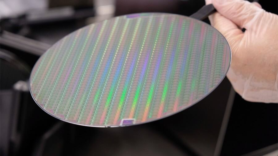
For now, NIST and Google do not mention which process technologies will be used, but SkyWater and Google already have an open-source 130nm process design kit (PDK) that can be used to design new chips or customize other open-source designs. Meanwhile, SkyWater offers 90nm and 130nm process technologies as well as has a qualified 65nm production node.
Interestingly, SkyWater will supply those open-source chips on wafers, which will require universities and other purchasers to dice them into individual dies, assemble them into appropriate packages, and test the final chips at their own processing facilities.
*University of Michigan, the University of Maryland, George Washington University, Brown University, and Carnegie Mellon University.

