Samsung plans big capacity jump for SSDs, preps 290-layer V-NAND this year, 430-layer for 2025
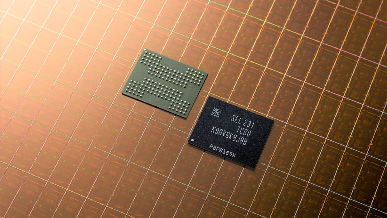
Samsung Electronics is set to begin mass production of its 9th generation V-NAND later this month, according to a Hankyung media report. The new generation of Samsung's 3D NAND memory will feature 290 active layers, which is hardly a significant increase from 236 layers, but this brings with it a substantial change in how these flash devices are made.
The report about 290-layer 9th Generation V-NAND contradicts Samsung's official plans to introduce 3D NAND memory with over 300 layers in 2024, so take the new information with a grain of salt. Meanwhile, it is possible that Samsung decided to reduce the number of active layers in its V-NAND memory to boost yields. Increasing yields at the cost of areal density may be a good way for Samsung to lower the costs of some of the best SSDs that it makes, particularly the drives for mainstream and low-cost systems.
A key feature of Samsung's 9th Generation V-NAND with 290 active layers is a string stacking production technique, according to the report. Manufacturing processes using string stacking involves building a CMOS layer with logic, then a 145-layer 3D NAND memory array on top, and then another 145-layer of 3D NAND flash above that. While this manufacturing technique is a complex one, it is poised to increase yields for 3D NAND memory products with hundreds of layers, as it is easier to build two 145-layer 3D NAND arrays than one 290-layer 3D NAND array.
Ultimately, the increased number of layers should enable Samsung to increase areal recording density of its 3D NAND devices. Increasing the density of 3D-NAND is a major goal for all NAND memory makers, as demand for flash in the industry is increasing. Increasing the number of layers in 3D NAND devices also increases production efficiency. Normally, makers of 3D NAND memory tend to increase the number of layers with every new node quite substantially. This may not be the case with Samsung's 9th Generation V-NAND with 290 layers, as it looks like this node will be primarily used to learn how to use string stacking in mass production. Also, it is possible that with 9th Generation V-NAND Samsung will also put more focus on 3D QLC NAND memory devices.
Looking ahead, Samsung has aggressive plans for maintaining its position in the 3D NAND flash market by introducing 3D NAND devices with an even higher number of layers, according to the report. Following the launch of the 290-layer V9, the company intends to release a 430-layer 10th generation V-NAND in the second half of 2025, the report says. This information is corroborated with last year's Blocks and Files report.
Meanwhile, other industry players are not far behind. SK hynix is gearing up to produce 321-layer NAND by early next year, while YMTC in China plans to manufacture 300-layer products by the second half of 2024, the report says.

