Intel's biggest failure pops up on a Pokemon-emblazoned motherboard — 10nm Cannon Lake rides in style on a custom Meowth board
The chip Intel wanted to hide the most keeps popping up in the oddest places. You may or may not have heard of Cannon Lake, but it was one of Intel's biggest busts. Cannon Lake was Intel's first 10nm processor to ship, arriving after years of delays while the company lost its manufacturing lead to TSMC and AMD, but it didn't actually work — Intel launched the defective chip in China only, effectively hiding it from the skeptical press as it looked to prove some form of life after years of delays, but the Cannon Lake chip came with a de-activated integrated GPU due to issues with the 10nm process. Intel also only released one version of the chip, while all other models were axed, relegating Cannon Lake to a notorious spot at the bottom of the chip industry's trash barrel. Intel's 10nm was broken, and it took multiple redesigns of the node before it became fit for purchase. Hardware enthusiast YuuKi_AnS takes us on a nostalgic trip down memory lane to revisit the 10nm Cannon Lake architecture with a look at a new oddly Pokemon-emblazoned board with the notorious chip.
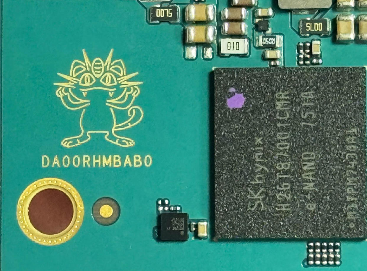
The memorabilia arrives as a compact motherboard with an integrated Cannon Lake processor. The motherboard is interesting, as there's a picture of the Pokemon Meowth on the bottom left corner of the PCB. We've often seen etchings on AMD and Intel processors, but this is the first time we've seen someone engrave a Pokemon on a piece of computer hardware.
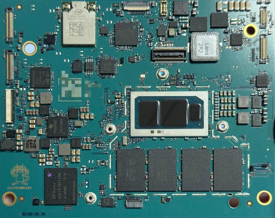
The engineering sample, potentially hailing from Lenovo, sports the Core M3-8114Y, a Cannon Lake-Y chip with a dual-core configuration with Hyper-Threading. The Core M3-8114Y is one of two known Cannon Lake processors that Intel developed. The other is the Core i3-8121U, which has a similar design but higher clock speeds. However, Intel only lists the Core i3-8121U on its website, disavowing the existence of the Core M3-8114Y.
In addition to the Core M3-8114Y, the motherboard houses 8GB of Samsung LPDDR4-3733 memory and 128GB of SK hynix eMMC storage. There's even Wi-Fi 5 connectivity, thanks to the onboard Intel 9560 (codename Jefferson Peak) wireless controller.
Cannon Lake features the BGA1392 package with dimensions of 28 x 16.5mm. The processors typically possess a two-die configuration. The CPU die, which measures 70.52 mm², is the more extensive die, followed by the smaller PCH die, which is 46.17 mm². However, the Core M3-8114Y has a unique design flaunting a third and smaller die. The 13.72 mm² die is suspected to be the McIVR (Multi-Chip Integrated Voltage Regulator) die, whose job was to regular the voltage between the two other dies.
Many obstacles prevented Intel from bringing Cannon Lake to the retail market. The architecture had suffered from one delay after another. There were some laptops with Cannon Lake chips, but they weren't widely available. Intel also used the Core i3-8121U in a couple of its Crimson Canyon NUCs, which the chipmaker retired in 2019. Having launched in 2018, Cannon Lake was one of Intel's most ephemeral architectures, even by the company's standards.

