AMD says the UCIe universal chiplet interface will create a whole ecosystem — custom multi-chiplet designs are the future
- Oops!Something went wrong.Please try again later.
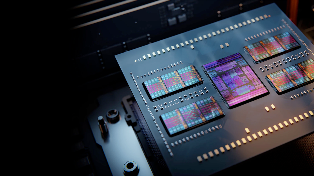
Several years ago, AMD adopted a multi-chiplet design for its client desktop and data center processors well ahead of its rivals. Back then, it was the only way for AMD to offer products with higher core counts than rival Intel, and now the move is seen as a strategic pivot towards an inevitable multichiplet design methodology. Today, Sam Naffziger, senior vice president and corporate fellow at AMD, thinks about how the Universal Chiplet Interconnect Express (UCIe) specification will create a chiplet ecosystem and enable custom multi-chiplet design.
For modular multichiplet designs, a high-performance, low-latency, and low-power interface is a must. The Infinity Fabric interface enabled AMD to build unique EPYC, Ryzen, and now Instinct MI300-series processors with unrivaled core counts, performance, and feature sets, Naffziger explained in a YouTube video conversation with Mark Papermaster, AMD's chief technology officer.
"The [interface] latency was too high, the power cost was too high, but we had a team of can-do engineers who said, 'I know how to solve that problem,' 'I will deliver a lightweight interface,' 'I will slim this down,' and 'I will eliminate cycles of latency,'" Naffziger said referring to the era when AMD was developing its multi-chiplet 2nd-gen EPYC and Ryzen processors. "If we hit these targets, now we have a multi-die solution that behaves just like a monolithic SoC. We set those targets, and then we oversaw the team's execution to make it happen. It was so transformative."
To a large degree, Infinity Fabric was a savior for AMD when it was introduced. However, since this is a proprietary technology, it cannot be used by third parties. This is where the open UCIe specification for die-to-die interconnects comes into play. The open spec, largely based on Intel's AIB, defines a 32 GT/s 16 to 64 lanes physical layer, protocol stack (CXL.io, CXL.mem, and CXL.cache), software model, and compliance testing procedures. As for performance, the UCIe 1.0 technology enables bandwidth density up to 1.35 TB/s per mm^2 for a common 45-micrometer bump pitch.
"What we can do [with UCIe] is have a chiplet ecosystem and library, […] UCIe opens up the opportunity for third parties to exploit that [modular design capability]," said Naffziger. "Companies who want to do a custom platform and leverage everything else can just do one little chiplet and bolt it up. So, the opportunities are endless. I mean this; we're going to see much more of this proliferating in the industry, but it does require standards and carefully thought-through design platform capability."
While AMD was part of the group that developed the UCIe specification, whether the company plans to build UCIe-compatible chiplets remains to be seen.

