Samsung's First 3nm GAA Chip Found in Cryptominer
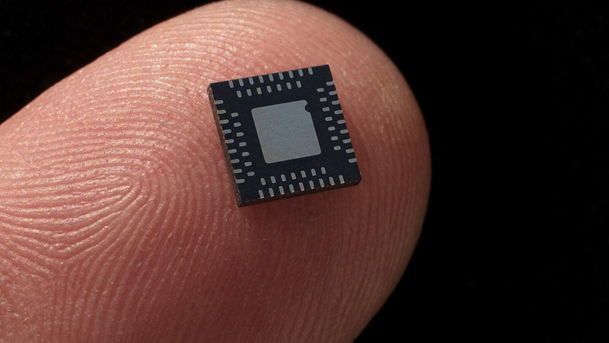
Samsung officially started high-volume production of chips on its SF3E (3nm-class, gate-all-around early) process technology about a year ago, but no fabless chip designer has ever confirmed that it uses this node for its products. But TechInsights recently discovered that MicroBT's Whatsminer M56S++ cryptominer has an application specific integrated circuit (ASIC) that is indeed made with Samsung's SF3E process.
ASICs used to mine cryptocurrency tend to be small devices with a relatively low transistor count featuring similar repeating logic structures and a minimal number of SRAM bit cells. This generally makes such chips, and the Whatsminer M56S++ in particular, very well suited for serving as pipe cleaners for the most advanced manufacturing technologies due to their production simplicity. For Samsung Foundry, it makes perfect sense to use its SF3E for chips like cryptocurrency mining ASICs.
Unfortunately, we do not know much about the Whatsminer M56S++ ASIC except that the MictoBT's mining machine based on this chip has a 240-256 Th/s hashrate and a 22J/T energy efficiency. For those interested in discovering more about the chip, we recommend buying an appropriate report from TechInsights.
Unfortunately, it is presently unknown whether Samsung's SF3E is currently used for applications beyond cryptocurrency mining chips. But officially, Samsung says that it makes products using its latest process node.
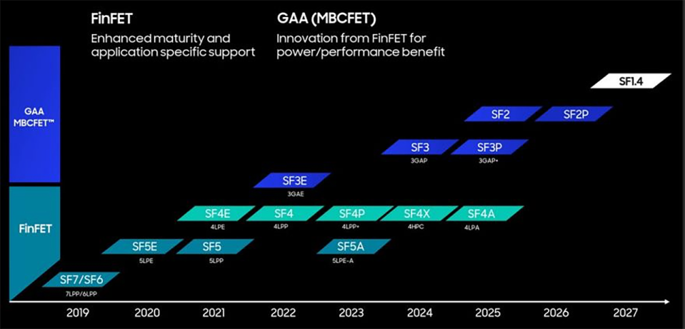
"We are mass producing the 1st gen 3-nano process with stable yields, and, based on this experience, we are developing the 2nd gen process to secure even greater mass production capabilities," a financial statement issued by Samsung reads.
When compared to Samsung's 2nd generation 5nm-class technology (SF5, 5LPP), SF3E (aka 3GAE) promises to decrease a chip's power consumption by up to 45% while maintaining the same complexity and frequency or it can enhance performance by 23% with similar transistor count and clocks. In addition, it can also reduce the area occupied by an integrated circuit (IC) by 16%. The company recently detailed its second-generation 3nm-class process called SF3.

