China Frustrated with Japan's New Export Rules Against Chip Sector
A day after Japan's new rules regarding exports of select wafer fab tools to China went into effect, the People's Republic issued a statement how frustrated it was with the move. A representative from the Chinese Foreign Ministry declared that this move appeared to be directly targeting China, and highlighted potential negative effects, including harm to businesses and disruption to the worldwide supply chain.
"China deeply regrets and is dissatisfied with the move, and it has made solemn representations to Japan at different levels," said Mao Ning, a spokesperson for the Chinese Foreign Ministry, according to a report by Nikkei. "We will closely monitor the impact of the regulatory policy and resolutely safeguard our own interests."
China urged Japan to focus on shared interests between the two nations rather than trying to restrict development of their semiconductor industry.
The statements made by the Foreign Ministry were more diplomatic than the somewhat aggressive language used by China's top envoy in the U.S. last week. The latter promised that Beijing would not hesitate to respond to further sanctions and export controls imposed by the U.S.
"We will not provoke, but we will not back down from provocations," Ambassador Xie Feng said during a forum, adding that China would definitely react.
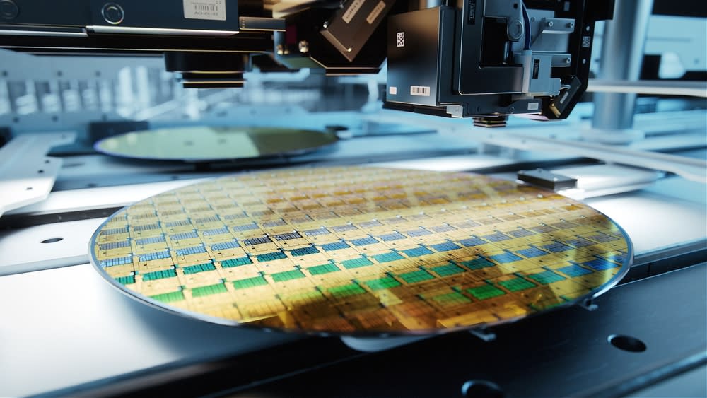
Japan's new export rules require manufacturers of wafer fab equipment to obtain an export license from the government before shipping any of 23 fab tools to a Chinese entity.
The list includes all immersion lithography scanners, etching equipment, tools for chemical wafer polishing, and extreme ultraviolet (EUV) mask-testers. Manufactured by ten companies such as Lasertec, Nikon, Screen Holdings, and Tokyo Electron, these additions to the export control list align with similar restrictions enforced against China by the U.S. and the Netherlands in recent quarters.
In particular, export rules require companies like ASML, Applied Materials, and Lam Research to obtain export licenses from their respective governments before shipping Chinese companies tools that enable them to make logic chips with non-planar transistors on nodes measuring 14nm/16nm or smaller, 3D NAND chips featuring 128 or more layers, and DRAM ICs with a half-pitch of 18nm or less.

